We are an award winning product design consultancy, we design connected products and instruments for pioneering technology companies.
The secret to scalable IoT products? PCB design and manufacturing
You can’t scale what you can’t build
Reading time 8 mins
Key Points
- 80% of IoT projects fail to scale—often due to overlooked hardware limitations, not bad ideas.
- PCB design and manufacturing form the backbone and blueprint of every connected product.
- Design for manufacturability (DfM) ensures your product can move from prototype to production without costly redesigns.
- Scalability in the real world means planning for more devices, more data, and more complexity—early.
- Outsourcing PCB design for IoT gives you access to deep technical expertise and accelerates development timelines.
- End-to-end PCB design and manufacturing partners help reduce development risk and improve product-market fit.
- Ignoring hardware strategy early leads to inflated costs, longer time to market, and product instability.
- Want to scale successfully? Ask experts with in-house capabilities for help, and start with a PCB designed to grow with your product
Ready to build smarter, scale faster, and reduce the risk without compromising quality? A custom PCB design is the foundation for making that happen!
Ben Mazur
Managing Director
I hope you enjoy reading this post.
If you would like us to develop your next product for you, click here
Brilliant ideas often die on the workbench—not because they lack innovation, but because they weren’t built to scale. For connected products, also known as IoT (the Internet of Things), industry surveys reveal that up to 80% of IoT products fail to meet their intended outcomes – 30% of which is due to scalability issues. These results highlight that going from prototype to production isn’t just a technical or financial challenge – it’s a strategic one. And the secret to getting it right starts with the often-underestimated foundation of every connected product: PCB design and manufacturing.
A printed circuit board (PCB) is more than just the mechanical base that makes an electronic device work. It’s the backbone and central nervous system that enables connectivity, controls performance, and determines whether a product is truly ready and able to scale. At Ignitec®, we’ve been designing and building custom PCBs for over a decade, supporting clients across aerospace, defence, medical, automotive, and environmental monitoring sectors. If scalability, optimised performance, reliability, and reduced development risks are what you’re looking for in the product you’re bringing to market, we’re here to help!
Scaling IoT isn’t linear – it’s exponential.
Moving an IoT proof of concept (PoC) into a market-ready product is one of the biggest hurdles in connected product development. Many prototypes perform well in controlled environments but fail to deliver at scale—not because the technology is flawed, but because the system wasn’t designed to grow. With connected products, scaling isn’t linear—it’s exponential. More devices mean more data, connections, and users—and far more complexity. Without a solid plan for network strain, data overload, overheating, latency, and device management, even the most promising projects can collapse under real-world demands.
This is why your hardware, firmware, and cloud architecture must be engineered with scalability baked in from the start—not retrofitted later. Schedule a free and confidential discovery call with an expert on our team to talk to you about our full-service range of flexible and affordable options.
Printed circuit boards (PCB) for beginners
Whether you’re launching your first IoT product or scaling an existing solution, understanding the role of the PCB in IoT is essential. We mentioned previously that a PCB is the backbone (physical support) and nervous system (conductor of electrical signals) of connected devices – referring to the functional and structural role it serves once built.
Simultaneously, the PCB is also a hardware blueprint with a design and planning role. It provides the architectural layout that determines how components are arranged, how signals flow, and how compact or manufacturable the device is:
- PCB design defines your product’s capabilities: Form factor, power consumption, wireless performance, and durability all begin at the board level.
- Cost and complexity scale with design choices: Poor layout decisions or unsuitable components can inflate production costs and delay your timeline.
- You need different boards at different stages: A prototyping PCB might work for a pitch or POC, but it needs re-engineering for manufacturability and certification.
That’s why involving a partner such as Ignitec® who understands both design and production is essential—especially in industries where compliance, reliability, and rapid deployment are crucial.
Why Design for Manufacture (DfM) in PCB projects matters early on
Did you know that 70% of manufacturing costs are determined in the design phase? One of the most common reasons IoT projects fail to scale is that the PCB wasn’t designed with manufacturing in mind. That’s where DfM—Design for Manufacture—comes in.
Designing with DfM principles ensures your product is:
- Ready for high-volume production with minimal redesign
- Optimised for testability and inspection
- Cost-effective and avoids expensive component swaps, rework and waste
- Built to meet compliance standards
- Facilitates automation
At Ignitec®, we embed DfM thinking right from the concept phase. We know how critical it is to design boards that function well and are easy and economical to produce at scale. The result? Fewer iterations, faster approvals, and smoother transitions from prototype to production. Call us for a quote!
Is outsourcing PCB design for IoT products the right call?
If your internal team is focused on UX, software, or core innovation, handling hardware design in-house can dilute your time and resources. That’s why outsourcing PCB design for IoT products is a game-changer—especially for startups and scale-ups. This is a strategic move that makes sense if:
- You lack in-house expertise in electronics design or DfM
- You’re working with tight timelines and need to accelerate development
- Your product roadmap involves certification, testing, or field deployment
- You want to avoid the trial-and-error costs of inexperienced design
At Ignitec®, our clients come to us not just for technical execution but also for our ability to bridge the gap between design, prototyping, and full-scale production. We bring your R&D vision to life with tested, reliable, production-ready hardware—without the guesswork.
What to look for in an end-to-end PCB design and manufacturing partner
When choosing an end-to-end PCB design and manufacturing partner, you’re not just outsourcing a task—you’re looking for someone you can trust to deliver that task on time, on budget, and above standard.
Here’s what to look for:
- Cross-functional expertise in electronics, firmware, and mechanical design
- In-house rapid prototyping, testing capabilities, and product manufacturing services
- Experience in scaling from early-stage builds to full production
- A proven track record across regulated industries
- Collaborative working style that integrates with your team and timelines
We’ve supported clients across regulated and mission-critical sectors, as well as Kickstarters looking for a jump-start—all equally important.
Ready to build to scale?
The success of your IoT product depends on more than just a good idea—it depends on designing, testing, and building it to scale. At Ignitec, we combine deep technical expertise with a strategic approach to product development, helping innovators like you bring reliable, commercially viable, and manufacturable devices to market. Please call us for more information.
Design for manufacturing results in products that are easier, faster, and more cost-effective to produce
Why you need rapid prototyping solutions for hardware innovation
Low Volume Manufacture – Specialised and Cost-Effective
FAQ’s
What is PCB design and manufacturing?
PCB design and manufacturing is the process of creating and producing printed circuit boards that connect and support electronic components. Design involves creating a layout that defines the board’s function, shape, and component placement. Manufacturing brings the design to life by fabricating and assembling the board with components.
Why is PCB design important in IoT products?
PCB design determines how compact, efficient, and scalable an IoT product can be. A well-designed PCB supports reliable connectivity, power management, and data processing in constrained devices. Poor design can lead to overheating, signal interference, or failure to scale.
How does design for manufacturability affect PCB projects?
Design for manufacturability (DfM) ensures that PCB designs can be efficiently and reliably produced at scale. It reduces errors, delays, and costs by aligning the design process with the realities of fabrication and assembly. Ignoring DfM can result in redesigns and production bottlenecks.
What is the role of a PCB in an electronic device?
A PCB provides the physical and electrical foundation for an electronic device. It holds components in place and routes electrical signals between them. It acts as both the device’s backbone and nervous system.
Which industries use custom PCB design and manufacturing?
Industries such as aerospace, automotive, medical devices, defence, and environmental monitoring rely on custom PCB design. These sectors demand high-performance, compact, and reliable electronic solutions. Custom PCBs allow for tailored functionality and strict compliance with standards.
Why do IoT projects fail at scale?
Many IoT projects are not engineered for large-scale deployment from the start. Scalability issues arise from poor PCB design, lack of planning for device density, and inadequate data handling strategies. These challenges often lead to system failure once the product is exposed to real-world conditions.
How do you move from PCB prototype to production?
Transitioning from prototype to production requires validating the design through testing, applying DfM principles, and choosing a capable manufacturer. Documentation, tolerances, and assembly plans must be refined. Skipping these steps can lead to costly errors during mass production.
What is involved in outsourcing PCB design for IoT products?
Outsourcing PCB design involves working with external experts to handle layout, simulation, and prototyping based on your product specifications. It allows access to specialised skills, tools, and experience that may not exist in-house. This approach is beneficial for startups and teams focused on core product development.
Why is scalability a concern in PCB design?
Scalability affects how a PCB can handle user increases, data flow, and device count without performance degradation. A scalable PCB design ensures consistency in performance across thousands of units. Without it, products may experience connectivity breakdowns or heat-related failures.
How can poor PCB design affect product development?
Poor PCB design can lead to signal interference, overheating, or non-compliance with safety standards. These issues delay development and increase costs through repeated testing and redesigns. If products fail after launch, they can also damage user trust.
What does end-to-end PCB design and manufacturing mean?
End-to-end PCB services cover the entire lifecycle from initial design to fabrication, assembly, and testing. This approach helps maintain continuity, reduce handover errors, and streamline timelines. It’s often preferred by teams developing complex or regulated products.
When should PCB design begin in a new product development cycle?
PCB design should begin early, ideally during the product’s concept and feasibility stage. This allows the design to align with mechanical, power, and connectivity requirements from the outset. Early integration also prevents costly rework later in development.
Why is DfM critical for PCB design and manufacturing?
DfM ensures the design can be produced reliably and cost-effectively using standard manufacturing processes. It accounts for spacing, material tolerances, thermal limits, and assembly methods. This reduces defects and increases yield in production runs.
Which challenges are common when scaling IoT hardware?
Common challenges include network congestion, data overload, heat dissipation, and increased power demands. These issues are often rooted in inadequate hardware and PCB design. Addressing them early is key to a scalable and stable product.
How does PCB layout influence product performance?
PCB layout affects signal integrity, electromagnetic interference, and power distribution. A good layout minimises noise and improves thermal management. It also enables smaller, more efficient products with longer operational lifespans.
What is the difference between single-layer and multi-layer PCBs?
Single-layer PCBs have one conductive layer and are simpler and cheaper to produce. Multi-layer PCBs have several stacked layers and offer greater functionality, density, and performance. Multi-layer designs are common in complex IoT and high-frequency applications.
How do you test a PCB before mass production?
PCBs are tested using methods such as automated optical inspection (AOI), in-circuit testing (ICT), and functional testing. These methods identify faults such as shorts, opens, and misaligned components. Testing helps ensure reliability and compliance before scaling up production.
Who is responsible for PCB manufacturability in product development?
Responsibility is typically shared between the electronics design team and the manufacturer. Designers must apply DfM principles while manufacturers provide feedback on production feasibility. Collaboration between both parties is essential for successful outcomes.
Why is thermal management critical in PCB manufacturing?
Poor thermal design can lead to overheating, reducing component lifespan and causing failure. Thermal management strategies include heat sinks, vias, and careful component placement. Effective heat control is critical in compact IoT devices that operate continuously.
How can early design decisions reduce time to market?
Good design decisions at the start—like choosing the right materials, layout strategy, and DfM practices—avoid costly revisions. They streamline prototyping, testing, and certification. This speeds up development and improves launch confidence.

Get a quote now
Ready to discuss your challenge and find out how we can help? Our rapid, all-in-one solution is here to help with all of your electronic design, software and mechanical design challenges. Get in touch with us now for a free quotation.
Comments
Get the print version
Download a PDF version of our article for easier offline reading and sharing with coworkers.

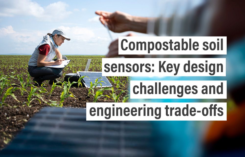
Compostable soil sensors: Key design challenges and engineering trade-offs
Are compostable soil sensors viable in the field? Explore the design challenges, power limits, and engineering trade-offs shaping biodegradable agri-IoT.
0 Comments