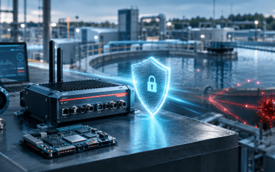
Across this series, we’ve examined eight distinct disciplines in defence electronics design: communications protocols, autonomy integration, secure updates, sensor power design, electromagnetic compatibility, radio selection, firmware security, and enclosure engineering. Each discipline, on its own, is well understood and well specified. What is less often discussed is the defence electronics interface risk: the failure mode that emerges not within any single discipline, but in the space between them, where two subsystems that each meet their own specification can undermine each other.
These gaps create vulnerabilities at critical boundaries (e.g., between legacy analogue components and digital processors, secure and unclassified networks, or physical hardware and cyber controls). This is where well-qualified platforms run into trouble in the field, and is the blind spot this closing piece sets out to address.
Defence Electronics Integration Failure Mode Scenario
Consider a reconnaissance UAV programme that completes its subsystem qualification on schedule. The enclosure passes its EMC and ingress testing. The radio passes its range and throughput trials on the bench. The power budget is signed off against the sensor payload’s expected duty cycle. Every discipline lead signs their section of the qualification report, and the platform goes to field trials.
In the field, the enclosure’s shielding, added late in the design to meet an EMC requirement against nearby jamming sources, sits closer to the antenna than the bench configuration used for radio testing. The link margin that looked comfortable on the bench is marginal in the deployed configuration. Around the same time, a firmware vulnerability is disclosed, and an over-the-air patch is issued. The patch is larger than routine sensor telemetry, and pushing it inside the power budget set for nominal sensor duty cycle means either delaying the patch or cutting into mission time. Neither option was in anyone’s spec.
Nothing here was a failure of engineering: The enclosure team met their EMC requirement, the radio team met their range requirement, and the power budget team met their duty-cycle requirement. The failure sits in the blind spot between the specs, not inside any one of them, and often surfaces at the exact moment where it’s most expensive to fix: after qualification and in the field.
Why do interface integration gaps persist?
It would be convenient to treat this defence electronics interface risk as a one-off oversight in a hypothetical scenario, but it isn’t. The structure of most defence electronics programmes makes this outcome likely rather than improbable. Requirements and architectures fundamentally mirror Conway’s Law phenomenon, where the structure of a system reflects the communication structures of the organisation building it.
In defence electronics, discipline-based decomposition (often broken down into Mechanical, Electrical, RF, Software/Firmware, and Optical) is necessary because of the specialised expertise, testing regimes, and distinct supply chains involved. A thermal and EMC engineer owns the enclosure spec. An RF engineer owns the radio and antenna specs. A power electronics engineer owns the energy budget. A firmware and security team owns update mechanisms. Each of these specialists is, correctly, focused on making their subsystem meet its own requirements as robustly as possible. The qualification process rewards exactly this: a clean pass against a defined test plan, signed and filed.
What the qualification process rarely tests directly is the interface itself, because the interface does not belong to any single discipline. Nobody’s job description says “own the relationship between enclosure shielding and antenna performance.” Nobody’s test plan says “verify OTA patch size against worst-case power budget under deferred maintenance conditions.” These are second-order effects of two first-order decisions, and second-order effects are structurally easy to miss when review gates are organised around first-order ownership.
This is not a criticism of any individual programme or supplier. It is a description of how specialisation works, which is, for good reason, how defence electronics gets built to the exacting standard it needs to meet. The point is not to abandon discipline-specific rigour: this rigour is necessary but not sufficient, as the gap between necessary and sufficient is where integration risk often resides.
|
⚒️DESIGN CONSIDERATION Subsystem qualification confirms that a component meets its own specification under its own test conditions. It does not confirm that the specification itself was set correctly against the conditions the component will actually operate under once integrated. The two are easy to conflate during programme reviews, particularly when schedule pressure favours treating a passed test as a closed risk. |
Pairing 1: Enclosure shielding and radio selection
The first post in this series covered rugged enclosures for defence electronics; another covered the process of choosing radios for defence deployments. When read separately, both are sound, but when considered simultaneously, a tension becomes visible that neither post, on its own, was positioned to raise.
Enclosure shielding decisions are typically driven by EMC and EMI requirements: protecting the platform’s electronics from external interference, and preventing the platform’s own emissions from creating a detectable or disruptive signature. These are legitimate, often mandatory, requirements, particularly in electronically contested environments. But shielding is not a passive addition. Conductive coatings, gasketing, and enclosure geometry all interact with whatever antenna is mounted on or near the enclosure. Depending on antenna placement and the specific shielding solution chosen, the result can be reduced radiated efficiency, altered radiation pattern, or a shifted resonant frequency relative to what the radio was tested against in isolation.
The radio selection process, meanwhile, is usually driven by range, throughput, spectrum availability, and power consumption requirements, tested against a reference antenna configuration that may or may not reflect the final enclosure design. If the enclosure design finalises after the radio has already been selected and bench-qualified, which is common when thermal and EMC requirements are still being resolved late in the design cycle, the radio is validated against conditions that no longer match the deployed configuration.
Neither team has done anything wrong. But the sequencing itself, radio qualification against a placeholder configuration, enclosure finalisation afterwards, creates a gap that only shows up when the two are tested together, which in many programmes happens for the first time at field trials rather than at subsystem qualification.
That being said, even when a defence procurement contract stipulates a Chief Systems Engineer or an Integration & Test (I&T) Lead whose job description is to “own the interfaces,” that role can, in practice, lack the technical authority or modelling tools needed to overrule discipline leads once schedules tighten.
|
⚠️CRITICAL ALERT Radio range and throughput figures qualified against a bench or reference antenna configuration should not be treated as final performance figures once the production enclosure and its shielding solution are locked. Re-verification against the as-built enclosure, not a representative or early-stage version, is the only way to confirm link margin holds in the deployed configuration. |
Pairing 2: Sensor power budgets and secure firmware updates
The second pairing sits between two other posts in this series: tactical sensor power design and secure over-the-air updates for defence IoT.
Power budgets for sensor platforms are typically set against a defined operational profile: sensing cadence, processing load, and communications duty cycle under expected mission conditions. This is sound practice, and getting it right is genuinely difficult, particularly on platforms where every gram and milliwatt is contested against payload, endurance, or weight requirements.
Secure firmware and OTA update mechanisms, covered previously in this series, are typically specified against security and reliability requirements: update integrity, rollback protection, and authentication overhead. These are non-negotiable in defence contexts for good reason. But secure updates are not free. Authenticated, verified OTA delivery consumes energy, both for the transmission itself and for the cryptographic processing required to validate it. In addition, the size of a security patch is dictated by the nature of the vulnerability being addressed, not by what fits comfortably inside the platform’s existing power budget.
When a critical patch needs to be pushed, and the power budget was set without headroom for exactly this scenario, the platform is left with an unplanned choice: defer the patch and accept the security exposure, or divert power from mission functions to accommodate it. Both are consequences of a decision that was, on paper, made correctly at the time, by two teams, each meeting their own requirements.
Real-World friction points in defence electronics integration
This gap is further exacerbated by real-world factors:
- The ‘Deferred Maintenance’ Trap: If a commander is told that updating a sensor array’s security patch will limit its tactical endurance, force a node to go offline to reboot, or reduce its battery life, they will almost always choose to defer the patch. This creates a massive, lingering cyber-vulnerability on the battlefield because the hardware couldn’t support the software’s hygiene requirements.
- The Radio Environment Penalty: If a sensor has to download a security patch in a contested electromagnetic environment, it will suffer from high packet loss. Retransmitting dropped packets means the radio stays in “transmit/receive” mode far longer than planned, compounding the power drain considerably.
- Silicon Limitations: Ultra-low-power microcontrollers used in defence sensors often lack hardware cryptographic acceleration. Doing heavy decryption entirely in software forces the processor to run at maximum clock speed for extended periods, eroding the thermal and power budget.
|
⚒️DESIGN CONSIDERATION Power budgets built against nominal or expected operational profiles rarely include a reserved allowance for unscheduled, security-driven OTA activity. Given that the timing and size of security patches cannot be predicted in advance, this is one of the few power budget line items that should be sized against a worst-case rather than an expected-case assumption. |
Pairing 3: Autonomy integration and degraded comms links
The third pairing connects the post on MAVLink integration in defence UAVs with the post on EMI and EMC in defence electronics, and it is arguably the least visible of the three because it surfaces as a software or autonomy behaviour rather than a hardware fault.
MAVLink-based autonomy and command-and-control logic is generally developed and tested against a comms link assumed to behave within a defined envelope: a certain latency, a certain packet loss tolerance, a certain reconnection time after a dropout. These assumptions are reasonable and necessary; autonomy logic has to be built against some defined link behaviour, or it cannot be built at all.
The EMI and EMC environment in which a platform actually operates in, particularly in contested or electronically dense environments, can push the comms link outside that envelope in ways that are transient rather than a clean failure. Latency spikes, intermittent packet loss, and brief link drops are not the same as a full loss-of-link event, and autonomy logic tuned around the clean failure case does not always handle the degraded-but-not-failed case gracefully. A platform can behave correctly during bench testing, correctly during a clean simulated link loss, and still behave unpredictably during the kind of intermittent degradation that EMI-heavy tactical environments actually produce.
As with the other two pairings, this is not a defect in either discipline. The autonomy logic was built against a defined link specification. The EMI environment was characterised and shielded against the relevant standard. The gap and defence electronics interface risk is that the autonomy logic’s assumptions about link behaviour under degradation were never tested against the EMI profile the platform is actually likely to encounter, because that test sits at the boundary between two disciplines and, again, belongs to neither by default.
Additional defence electronics interface risks worth naming
The three pairings above are illustrative, not exhaustive, as it would be misleading to imply these are the only interfaces worth scrutinising. A few others are worth flagging briefly, even without the full treatment given above.
Enclosure and power interact through thermal management, not just shielding: an enclosure sized primarily for EMC and ingress protection can constrain airflow in ways that push power electronics closer to their thermal limits, independent of the radio-shielding question raised in Pairing 1. Secure firmware updates and autonomy logic interact around timing rather than power: an authenticated update process that briefly interrupts command-and-control communication can collide with autonomy logic that was never built to expect a comms interruption at that particular moment in a mission, a distinct failure mode from the degraded-link case in Pairing 3. And spectrum and radio selection decisions interact with EMC in the opposite direction from Pairing 1: a radio chosen primarily for range or throughput can itself become a source of emissions that the platform’s own EMC design then has to absorb.
Each of these defence electronics interface risks sits at a different boundary to the three pairings developed above, which is the point worth taking from the list: the same subsystems can generate more than one distinct interface risk, depending on which property, thermal, timing, or emissions, is under strain at the boundary.
What this means for defence electronics engineers
For engineering teams, the practical implication is not a call for less specialisation. Deep discipline expertise is exactly what makes each subsystem reliable, and nothing in this post is intended to suggest otherwise. The implication is that interface conditions need to be treated as first-class requirements in their own right, explicitly owned by a specific role, rather than assumed to fall out correctly once each discipline has independently met its own specification.
Concretely, this requires shifting three standard practices:
- Qualify against reality, not reference: Test radio performance against the as-built enclosure rather than an idealised reference configuration. Crucially, this must happen late enough in the programme that the physical enclosure design is genuinely final.
- Account for the cyber tax: Treat worst-case, security-driven OTA activity as a defined line item in the power budget, rather than an unplanned draw against a general margin set for operational runtime.
- Enforce cross-discipline questioning: At every design review, force a version of the same question: What does this subsystem decision assume about the adjacent subsystems it touches, and has that assumption been checked against where those teams actually landed?
What this means for acquisition leads and decision-makers
For programme managers and procurement teams, the implication is about where risk is reviewed, not just where it is specified. A qualification process organised entirely around discipline-specific test plans will, by construction, miss interface risk, because interface risk does not belong to any single test plan. This is not an argument for more testing in general; it is an argument for a specific, additional category of review: cross-domain interface checks, positioned deliberately at the boundaries between disciplines, with clear ownership assigned rather than assumed.
In practice, this can be as straightforward as a review gate that asks, explicitly, which subsystem pairs have interdependencies that haven’t yet been tested together, and ensuring that the gate is scheduled late enough in the programme that the answer reflects final, not placeholder, configurations on both sides. It is a modest process addition against the cost of discovering the same gap during field trials or, worse, after fielding.
Final thoughts on the limitations of modern tooling for defence electronics
The industry is acutely aware of these defence electronics interface risks and blind spots, pouring billions into solutions like Model-Based Systems Engineering (MBSE) to digitally simulate second-order effects, Digital Twins to test edge-case power scenarios, and Lead System Integrator (LSI) contracts to assign explicit interface ownership. And despite this, these tools frequently fail to bridge the gap.
The reason is straightforward: a digital twin or an integration contract is only as good as the human processes surrounding it. If review gates still prioritise siloed, first-order compliance, no amount of advanced modelling software will force an engineer to look across the boundary of their own discipline. True integration doesn’t start with better tools, but by treating the interface itself as a non-negotiable requirement.
|
WORK WITH IGNITEC If your programme’s qualification process is organised strictly by discipline, an independent cross-domain review of your platform’s highest-risk subsystem interfaces, before field trials, not after, is one of the most cost-effective risk reductions available at this stage. |
Our engineering team works across the communications, power, security, and mechanical disciplines covered in this series, which is precisely the combination needed to identify these gaps before they reach the field. Book a free consultation with an expert on our team to ensure your defence project meets its strategic ambitions.